|
|
|
||||||||||||||||||||||||||||||||||||||||||||||||||||||||||||||||||||||
|
|
|||||||||||||||||||||||||||||||||||||||||||||||||||||||||||||||||||||||
|
|
|
||||||||||||||||||||||||||||||||||||||||||||||||||||||||||||||||||||||
|
The ANFF is
an open access network comprising of eight Nodes across 21 institutions with
a portfolio of more than 500 tools valued at over $200 million. See: for full details |
Coatings
Information
This page holds general information on coating
design and deposition technology, and specific information related to the
tools, processes and materials in use at Optofab
ACT where standard processes are established. Coating design software, tips,
and materials data Available materials in Spector
IBS Coating properties: Thickness dependent film properties Coming later: Coating Adhesion Particulates and cleaning OH contamination Interfacial absorption More Coating
Design Methods and Software
Optofab
ACT has a suite of design and modelling software for interference coatings and
can perform design to specifications as part of our service. Some users may
however wish to investigate coating design on their own and supply a
suggested recipe for their desired device. Here we provide some links to
appropriate design resources and materials properties for our calibrated
processes. However please note that the final refractive indices etc are not
those present inside the coating tool due to annealing and stress relaxation
and we will always have to modify the design for deposition monitoring
purposes so we can program the layers appropriately to account for these
changes and also to enable optical monitoring. All supplied designs will also
have to be run through our software suite to determine the tolerance budget
and optimised for this if necessary. Coating design is well studied and there are a
number of good books on the topic, for example see: http://www.sspectra.com/literature.html The book Design of Optical Interference Coatings
by Alfred Thelen was kindly made available free of
charge by the author for some time, you may be able to find a freely
downloadable copy of it. This book and others provide a conceptual framework
for interference coating designs of pretty much all the usual kinds. Having
then a framework, software is needed to tailor the starting design to the
required specifications. There is free code available to do this from the
Polytechnique de Montreal called OpenFilters, see: https://www.polymtl.ca/larfis/en/links This is quite a capable program, though it lacks a
little integration and cannot optimise designs with tolerancing in mind as
some of the commercial products can. Python source code is also available
under the GNU public license arrangements so you can modify it to suit if
suitably inclined and motivated. We run it at Optofab
ACT as it can be available everywhere, and also to have a common base for
design exchange with our customers. We have a range of custom written Labview code for converting materials files, creating
design templates, etc for Openfilters
that will be made available for Download shortly. Beyond this, there are many
commercial options. An incomplete list of some of the more commonly used
programs is presented below: TFCALC free version available with limited materials Filmstar free version with fixed refractive indices Freesnell free We use TFCALC routinely, and will invest in Optilayer once we have the broadband monitoring systems
running as Optilayer has a module that enables on
line correction/compensation to still meet spec if a layer is incorrectly
deposited or terminated, and it supports both broadband and ellipsometric monitoring. Before leaving the topic it is also worth
mentioning that with any of these optimising software models, how you set the
targets is critical to the convergence to a practically useful result. On the
one hand you want to use the minimum number of target points to maximise
iteration speed, but on the other oscillations in the response mean that
being too sparse or having the target points at the wrong wavelength will
generate designs that are not what is desired with peaks/troughs not caught
by the target points. Therefore measures need to be taken to prevent this
(for example stop the optimisation and look at the response and adjust the
target wavelengths to the peak/trough positions). Another issue is just putting in very simple
targets. For example, there may be a need for a mirror with very high 1064 nm
reflectivity and a very tightly controlled 532nm partial transmission. It is
tempting to put in targets at just 1064 and 532nm and run the optimiser. This
can produce results with steep slopes at the target wavelengths that are then
very fabrication sensitive. Better to put in three points at each target
wavelength, one at the wavelength and one either side with carefully chosen
values to try to force the software to make a peak or trough there which will
be more fabrication tolerant. Similar principles apply to bandpass
or edgepass filters where extra points should be
used to control the roll off shape to enhance fabrication tolerances. Our standard IBS coatings use Silica and Tantala as the low and high refractive index coatings
respectively. We run two processes, one at 150C deposition temperature with a
post deposition anneal to stabilise the coating and reduce absorption, and
one at room temperature with the assist gun to reduce stress and avoid high
temperature anneals which the target device (e.g. a deformable mirror) may
not be able to tolerate. Representative post anneal or post deposition
dispersion curves for the materials are provided below (shortly) for the
standard single rotation case, but we note that the precise behaviour of
index and stress and layer thickness changes on annealing are subject to the
exact coating design due to stress distributions through the coating and the
change in sign of the Tantala stress during anneal.
For dual position single rotation depositions, contact us as this case is
more complex.
Available
materials and typical coating rates - IBS
As the IBS system uses 14 water cooled targets
that can cost up to USD15k, then we only hold a limited number of them. The
currently available materials are:
Currently Only Silica and Tantala
are properly characterised. We are happy to attempt others but are not yet
able to guarantee performance with them. The metal targets can also be sputtered in the
presence of nitrogen to form the corresponding nitrides, but we have not yet
developed processes for this. As noted under the tool capabilities, the IBS
system is restricted purely to depositing metal oxides and nitrides and
whilst fluorides are possible in the presence of NF3, we are not going to
contaminate the chamber by doing this. Additional targets can be purchased as
required for coating jobs, though if these are very expensive and it looks as
if the material in question is very specialised, additional charges may
apply. The targets in the tool as standard will be Silica, Tantala, and Titania, and in the long run target change
costs will be applied as its about an hours work to change a target.
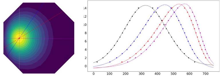
Deposition profiles and rates have so far only been characterised in depth
for Silica and Tantala. The image below shows a
typical deposition rate distribution measured at the deposition plane for Tantala, and for the standard single rotation cases the
deposition rates are ~0.1 nm/sec
for Silica and Tantala at 100C substrate
temperature.
The deposition rates are very stable over time,
and thick coatings can be deposited though obviously this takes quite some
time and will cost rather more. Coatings of 10-20 microns thickness are
entirely viable (subject to stress constraints for 150C coatings), just slow.
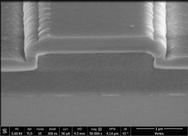
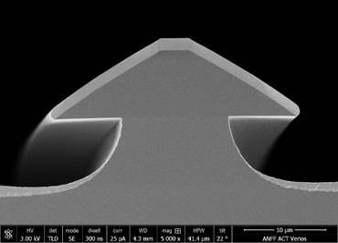
For the standard single rotation deposition, the coating can be quite
conformal, the images below showing coatings over steps of sizes as
indicated.
Uniformity
Two types of depositions are possible: ·
single rotation depositions where a plate holding
the substrates is located in a fixed position (which can easily be changed)
and rotated about its centre ·
Dual rotation where the rotating substrate plate
is sequentially positioned at two different locations for each layer to put down
two complementary profile parts of each layer that sum up to a high
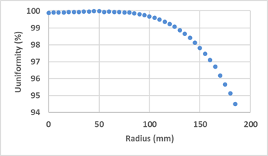
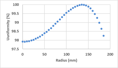
uniformity layer over a large area. For single rotation films, the uniformity pattern
depends on the position of the substrate holder, and results from modelling
are shown below to indicate the range of possibilities which allow for
optimising maximum area, PCD for a given substrate size, or flatness. It is
also clear from these plots how two complementary positions can be found for
the dual rotation case to absolutely maximise uniformity over large areas.
Typical measured thickness uniformity results for
each type of run are shown below and reflect that the modelled data
represents reality reasonably well:
Single rotation uniformity plot at different
positions showing maximum single substrate flatness or largest PCD for many 1
substrate deposition
Dual rotation showing large diameter high
uniformity Single rotation is much simpler, faster, and lower
cost and sufficient for small substrates where ~0.1% uniformity can
theoretically be achieved on many substrates in one run up to 50mm diameter.
For substrates beyond 100mm diameter (only 1% uniformity possible for runs of
up to 6 substrates in single rotation or better with fewer substrates on
smaller pitch circle diameter, see above uniformity data), it may be necessary
to go to dual rotation which is rather more complex and expensive but that
can offer sub 0.1% uniformity under optimal conditions on 400mm diameter
substrates. Repeatability
The typical run to run repeatability in thickness
uniformity characterised by the standard deviation on the total number of
runs for Silica and Tantala are respectively 3.5 %
and 3 %. It is important to note that deposition rate and
uniformity vary with the plume shape and hence strongly depend on the grid
set. As our initial grid sets are of unknown heritage we are currently
sourcing several new grid sets of nominally the same specification to improve
the grid set dependence. More details when we have them
Uniformity shape depends on grid set and wear Absorption
Absorption losses in annealed coatings are very
low, typically <10ppm in coatings up to 5 microns thick. This means
extremely high reflectivities and many pass mirror
cells are very possible with IBS coatings. We are currently analysing the
absorption loss in detail by depositing Silica or Tantala
onto high Q factor disk resonators and looking at the Q as a function of
annealing temperature to characterise this in great detail. Initial results
for all loss sources combined (absorption, surface scatter, volume scatter)
have the Tantala at 0.1 dB/cm at 1550nm, and the
Silica at 0.05 dB/cm. For silica this equates to 1.1 ppm total loss per
micron of coating thickness at 1550 nm. This study will be ongoing and will
look at other wavelengths over time, check back later for more data Coating Stress
IBS coatings are deposited with considerable
kinetic energy as the typical ion energies before neutralisation and target
bombardment are in the 1000eV range. It is this energetic nature that gives
them their densely packed environmentally insensitive nature. However, this
also produces considerable compressive stress in the as deposited coatings.
We have quantified the coating stresses by measuring bow on silicon wafers. Assuming the thicknesses of the substrate and the
coating are smaller than the lateral dimensions, thickness of the coating is
smaller than the thickness of the substrate, the substrate and coating are
homogenous, the radius of curvature is equal in all directions (spherical
deformation), the thin film residual stress (s)
can be deduced from the radius of curvature (R) measured before and after
deposition of the film thanks to the Stoney formula (Ardigo M., Ahmed M., Besnard A. (2014). Stoney Formula: Investigation of
Curvature Measurements by Optical Profilometer. Advanced Materials Research.
996. 361-366).
Es is the Youngs
modulus of the substrate n is the Poissons
ratio of the substrate ts is the substrate
thickness, tf is the film thickness R1 is the radius of
curvature before deposition (substrate) R2 is the radius of
curvature after deposition (substrate + film) The measurement of the radius of curvature is
realized with a Dektak 504 profilometer
that gives a direct access to the sagitta (Z)
of the measured sample from which R can be deduced.
Where L is the total scan length. The substrates
used are 4 wafers Si [100], 525 m thick, p type, the scan length is 55mm. The bow
measurements are done on the bare Si substrate first, then on the Si
substrate with the deposited film and finally on the annealed Si substrate
with the deposited film. The standard IBS Ta2O5 films
deposited in the Spector have a typical compressive -195MPa residual stress
as deposited that becomes tensile +52 MPa after standard annealing. The
standard IBS SiO2 films deposited in the Spector have a typical
compressive -551 MPa residual stress as deposited that stays compressive at
-184 MPa after standard annealing. We are also
currently starting to investigate low stress coatings. This can be achieved
by low temperature deposition and by using the assist ion gun running on
oxygen. Data will be presented when studies are complete.
Thickness
Dependent Film Properties
Index of Refraction VariationThe refractive index of
an optical coating depends on a combination of many parameters. Besides stoichiometry,
the deposition method as well as thermal history affects the optical
properties of the final product. For ion beam sputtered coatings, the
variation of beam current, particle energy, direction of travel, substrate
temperature, process pressure, background atmospheric composition, and
interaction with intra-vacuum objects can all lead to inhomogeneities of the
coatings. When ultimate precision is required over large apertures, even
small variations can compromise reflective or antireflective coating
properties.
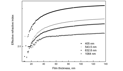
There is also the
question of homogeneity within a layer. With techniques such as e-beam
evaporation it is well known that the initial part of a film (first 20nm or
so) has different properties to the later part. We have not yet characterised
this for the Spector IBS, but data exists to suggest similar effects apply
certainly to Tantala layers, for example the data
below from CSIRO for Tantala for a film as it grows
plotting the effective index vs film thickness.
|
||||||||||||||||||||||||||||||||||||||||||||||||||||||||||||||||||||||


Pulse Duration
|
<
1ns
|
1ns-100ns
|
100ns-100ms
|
>100ms
|
Damage Mechanism |
Nonlinear ionisation |
Dielectric Breakdown |
Thermal and dielectric breakdown |
Thermal |
Relevant damage spec |
Ultrafast specific |
Pulsed |
Pulsed and CW |
CW |
There are also wavelength effects (most materials exhibiting
enhanced absorption at DUV and MIR wavelengths) and Beam profile effects
through the peak intensity present in the beam at a given power level e.g.
Gaussian has twice the intensity of flat top of the same power.
Thermal effects are driven by absorption in the
coating materials themselves or the substrate, or from defects in the coating
and lead to heating of the coating and eventual melting, stress induced
coating pop off, or recrystalisation. For a
Gaussian beam heating a coating by surface absorption, the temperature rise
is given by:

Where bs
is the surface absorption, P is the power, k is the thermal conductivity, k is the thermal diffusivity, tI
is the irradiation time, w is the 1/e2 beam diameter. When
the irradiation time is long compared to the thermal diffusivity time
constant (w2/k) the above equation has an asymptotic solution given by:
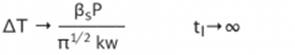
Note that counterintuitively
this is characterised by P/w ie W/cm and not
intensity (W/cm2). Thus the CW and long pulse damage threshold has
linear scaling with power and beam diameter.
For shorter pulses the full
equation has to be solved and there is a cross over zone where thermal or breakdown
damage or a combination of both occurs. In this zone it is common practice to
express the LIDT in fluence (J/cm2), which again is
counterintuitive as there is then no time dependence in the specification
which certainly exists in practice. A better spec is in intensity (W/cm2).
However, as the ultrashort
pulse regime is entered, a range of nonlinear effects come into play and a
totally separate damage specification is required for this. In the best
possible case, damage here is defined by the ablation threshold of the
materials, e.g. about 2 J/cm2 for silica at 1030nm with pulses of
a few hundred femtoseconds. There are a wide range of things that can lower
this such as electric field enhancement around defects in the coating or on
the substrate surface, doping of the materials, photochemically deposited
atmospheric materials, photodarkening, etc.
As noted, the wavelength
matters, and in the absence of detailed data, the damage threshold is usually
assumed to scale inversely with wavelength as long as no absorption bands are
encountered. As a single pulse duration is normally only given for the pulsed
damage threshold, then as long as the pulse you are interested in is not in
the ultrafast regime, the scaling based on the square root of the ratio of
the pulse durations is usually applied for pulse lengths below 100ns. Above
100ns, the thermal effects come into play and scaling is more difficult to
predict but some idea may be obtained from comparing the predicted LIDT for
100ns with that from the CW regime.
IBS coatings are restricted in
our system to metal oxides and nitrides on the whole and in the 400nm to
potentially 4m
region have very low linear absorption if correctly deposited and thermally
annealed. To give some concrete numbers, as noted previously early
measurements for all scattering and absorption losses summed indicate 0.05
dB/cm loss for silica at 1550nm (1.1 ppm per micron), and 0.1 dB/cm for tantala (2.2 ppm per micron) as measured by waveguide
propagation losses by coating very high Q disk resonators with ~2 micron
thick films. As the light is now propagating through the film rather than
perpendicular to it, then as well as absorption, this figure also includes a
significant surface scattering loss that would not be encountered in a
standard transmissive or reflective thin film filter stack. We have not yet
measured LIDT on these coatings, but expect them to be high. Data will be
provided once available.
DUV and MIR are usually the domain
of IAD E-beam coating. We do not yet have this system running and so have no
figures for these regions.
A
coating method for every application
Optical coatings can be deposited by many methods, each having its own characteristic strengths and weaknesses. Here we provide some generic but detailed information on the usual suspects
Ion assisted E-beam
evaporation
Chemical Vapour Deposition
(PECVD, APCVD)
Fast Atomic Layer Deposition
(ALD)
Coating
Methodologies
E-Beam
evaporation
E-Beam or Electron beam evaporation is a type of
Physical Vapour Deposition process where target material is bombarded with an
electron beam through charged tungsten filament under a high vacuum process
chamber. The electron beam causes the atoms from target material into gaseous
state and then precipitating into the solid form coating onto the substrate
inside the vacuum chamber within the line of sight. The electron beam is
generated by an electron gun, which produces thermionic emission from the
tungsten filament and emitted electrons are accelerated by high voltage
potential (kilovolts).
The advantage of E-beam coating is the deposition rate
of this process ranges from very low (1 nm per minute) to very high (few
micrometres per minute) making the material utilization efficiency very high
and it also offers structural and morphological control of the film with very
high thermal efficiency, high productivity and low contamination. The
deposition rate can be measured using in situ by quartz crystal and
deposition rate depends on the starting materials and E-Beam power.
The electricity density of the electron beam is
very large and deposition of various materials is possible like high melting
points, oxide materials and materials which sublime. It is possible to have
multiplayer film coating using several sources and crucibles in the process
chambers.

Fig.1:E-beam operation principle
Ion
Assisted E-Beam evaporation
During the Ion assist E-beam operation, an ion
beam typically from argon gas with broad range of energy is targeted towards
the substrate and it arrives alongside the evaporant
materials to be deposited. The directed Ions impart the energy into atoms of
the evaporant materials and increases the surface
mobility. The surface mobility of the atoms helped the materials to improve
the adhesion, density and structure of the thin film. Because of these
improved film quality, this technique provides more repeatable refractive
index of the material.
Ion assist E-beam evaporation can be achieved by
typically using End-hall type of Ion source which provides uniform substrate
coverage and control over the current and energy of the Ion beam.
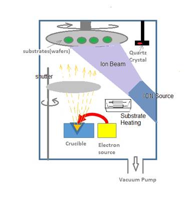
Fig.2:Ion Assisted E-beam operation principle
Reactive
Magnetron Sputtering
Magnetron Sputtering process is another type of
Physical Vapour Deposition (PVD) technique to grow thin films on to the substrates
because large quantity of films can be produced with relatively high quality
and low cost. The magnetron sputtering process involves a gaseous plasma
which is generated by introducing inert high molecular weight sputtering gas
like Argon or xenon and confined to a source where material target is
located. The high energy ions of the plasma erodes the surface of the target
and ejected atoms travel through the Vacuum environment and deposited on to
the substrates to form thin films.
The plasma is initiated by applying a high voltage
between the cathode (located behind the target) and anode (commonly connected
to the chamber as ground).Electrons from the sputtering gas are accelerated
away from the cathode and collide with the nearby atoms from sputtering gas
resulting an electrostatic repulsion which knocks off the electrons from the
sputtering gas atoms causing ionisation.
The positively charged atoms now accelerate
towards the negatively charged cathode causing high energy collisions with
the target materials. Each of this collision eject atoms from the target
materials with good enough kinetic energy to reach to the surface of the
substrate start to condense to form a thin film. As more and more such atoms
combine together on the substrate, they start binding each other at molecular
level forming tightly bound atomic layer. A precise layer of thin film is
created by producing one or more such atomic layers depending on the
sputtering time.
There are different type of magnetron sputtering
such as DC magnetron sputtering and RF magnetron sputtering each having
different working principles and objectives.
The advantage of RF magnetron sputtering over the
DC magnetron sputtering is, it does not require the target as an electrode to
be electrically conductive hence any material can be deposited theoretically
using RF magnetron sputtering.
In case of standard sputtering, a target of
whatever pure material is desired and an inert gas usually an argon is used.
However in the reactive sputtering, non-inert gases such as oxygen or
nitrogen is used either in place of or in addition of inert gas(Argon). In this case the ionised non inert gas
chemically react with the vapour of target materials and form a compound
molecular layer which is deposited as a thin film on to the substrate.For example a silicon target with non inert gas oxygen can form Silicon di oxide layer or
with N2 can form Silicon nitride layer.
In many cases it is also possible that the reactive
gas ions chemically react with surface of the target materials and does not
sputter anything from the target.This state of the
target is called poisoning state.To get a good film
stoichiometry with high deposition rate requires the target material state to
be in fixed state between pure metallic and pure oxide materials.


Fig.3:DC sputtering system Fig.4: Magnetron sputtering system
Ion
Beam Sputtering
Ion Beam Sputtering is one of the PVD methods
which provides very fine and good quality thin film coating. During the Ion
beam deposition, Ions from the Ion source is focused on the Target materials
and the sputtered material from the target is deposited on to the substrate
as a thin film. The system configuration may include another guided ion
source, which focuses the ion beam directly to the substrate assisting highly
dense film deposition. Although in the typical IBS system, the main feature
of the system is Ion source, a target and a substrate. The system
configuration with extra guided ion source is known as Ion Assist Deposition.

Fig.5:Ion Beam Sputtering(Ion assist)
Ion Beam deposition method is one of the slowest
and most expensive deposition method but it produces very high quality film
with good precision.
Chemical
Vapour Deposition (PECVD, APCVD)
CVD is a versatile deposition technique that
provides the process of growing thin films of elemental and compound semiconductor
materials, amorphous or crystalline compound and metal alloys of different
stoichiometry. It consists of chemically reactive volatile compound of the
materials to be deposited with other gases to produce non-volatile solid on a
suitable substrate as an atomic layer.CVD process
is a very well established technique and the reactor or process chamber used
for the process mainly depends on the precursor, condition of the deposition,
kind of energy used to the system to activate the chemical reaction. The
following processes are the most established CVD processes in the industry:
-
PECVD-Plasma Enhanced Chemical Vapour
Deposition(When plasma is used to introduce chemical reactions i.e. Microwave
or RF power based plasma)
-
APCVD-Atmospheric Pressured Chemical Vapour
Deposition(It is a CVD process which uses atmospheric pressure to provoke
chemical reactions)
-
LPCVD-Low Pressure Chemical Vapour Deposition(CVD
process at low gas pressure of 0.6 to 1.33mbar)
-
MOCVD-Metal Oxide Chemical Vapour Deposition(In this
process of CVD the metal oxides are used as precursors for example trimethylaluminium, trimethylgallium)
There are two type of typical CVD reactors, hot
wall CVD and cold wall CVD. In the hot wall CVD, the heating is achieved by
surrounding the resistive element around the reactor and in the cold wall
CVD, the substrate holder is heated up while the chamber walls are air cooled
or water cooled.
PECVD(Plasma Enhanced Chemical Vapour Deposition)
PECVD is a very common and well established CVD process
which uses much lower temperature than the typical CVD process to deposit
various materials from gas state to a solid state thin film on to the
substrate. In this process deposition is achieved by introducing reactive gas
between two electrodes one is grounded and another one is RF powered (or AC
frequency or DC discharge). The plasma is created by the capacitive coupling
of two electrodes which induces a chemical reactions resulting a product
being deposited on to the substrate. The substrate which is mounted on the
ground electrode is typically heated at 250C to 350C depending upon the
specific thin film requirement. During the PECVD process, the electrons
acquired sufficient energy from the applied electric field to create reactive
species without increasing the gas temperature in the process chamber. And
this is the key advantage of PECVD maintaining the lower temperature process
comparing to other CVD methods.
The energised electrons and gas molecules collide
to each other in plasma and decomposes the source gases to form the reactive
species such as excited neutrals and free radicals as well as ions and
electrons. PECVD could be operated using RF (13.56Mhz), AC (50Hz), Microwave
(2.45GHZ) or DC power supplies, with RF being the most common source of power
supply in most of the PECVD system.
For example, to deposit silicon di oxide (SiO2)
film, the plasm decomposes the silicon gas sources SiH4(Silane),Tetramethoxysilane(TMOS) or HMDS to silicon radicals and reacts
with O2 radicals from oxygen sources or N2O sources inside the vacuum
chamber. When the RF power is applied to generate the plasma, the energised
electrons ionise the reactant gases and create more chemically reactive
radicals which react to form thin film materials on top of the substrate or
sample. The vacuum chamber (Fig.5) is connected to pump system which consists
of roughing pump and Turbomolecular pump to pump down the chamber to very low
vacuum level. The gas system is connected to the chamber through Mass flow
controller. The MFC controls the flow rate of the gas inside the chamber. As
mentioned above the plasma is ignited by applying electric field at RF
frequency from RF sources.
Various kind of inorganic films are produced using
the PECVD system in semiconductor or photonics industry such as SiO2, Silicon
Nitride, Silicon Ox nitride etc.
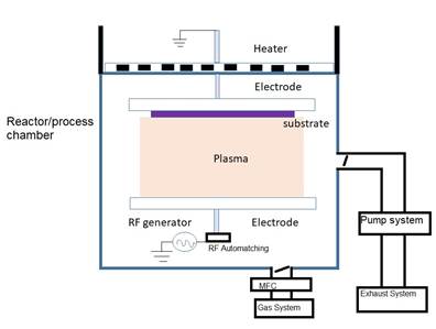
Fig.6:PECVD System
APCVD(Atmospheric Pressure Chemical Vapour Deposition)
APCVD is a CVD method which deposits different
kinds of oxide materials (doped and undoped) at atmospheric pressure. This
process is highly suitable for volume production, continuous in line
manufacturing, etc as it is vacuum free and can coat many substrates on a
belt feed or long rolls of material. It is often used in low cost production
like PV cell manufacturing.
APCVD process can be used for the following
applications:
-
Production of compound semiconductors
-
AR coatings on glasses and lenses
-
Silicon-di-oxide and Transparent Conductive Oxide
(TCO) coatings.
Some of the Transparent Conductive Oxide coatings
are on flat panel displays like OLED, LCD, touch screen, solar cells etc. High
temperature APCVD process is used for producing thin film in many other
technologies like solid state devices, metal oxide semiconductors, graphene
based devices and APCVD is one of the best to produce graphene.
Fast
Atomic Layer Deposition
Atomic Layer Deposition (ALD) is a type of vapour
phase technique used to deposit thin film layer onto the substrate.ALD
can produce defect free and angstrom level controlled films. It is a gas
phase method based on sequential and self-limiting surface reaction process
where each reaction allows only one monolayer of deposition. The nature of
interaction between the precursor and surface determines the complete cycle
of ALD. Depending on the requirement, the ALD cycle can be performed multiple
times to increase the layers of thin films. The process of ALD can be
performed in lower temperature very often which is beneficial for the fragile
and thermally sensitive materials. With the emergence of nanotechnologies and
electronics miniaturisation, the application of ALD has become very popular
and vast in terms of coatings nano layers and thin
films. In ALD process, gas phase reactions are prevented by injecting the
precursor separately and as a result it allows self-limiting reactions on the
surface of the substrate. Defects free films are deposited on the substrate
comparatively at low temperature using ALD allowing the low-temperature
processing as key requirement by some technology manufacturing like display
coatings.
However throughput is very low in this case due to
the long cycle duration of ALD cycle which is approximately 10sec or more at
lower temperature.
To meet the high volume industrial production and
throughput, spatial kind of ALD is developed where precursors and reactants
are continuously injected into different spaces, using different distinct
zones separated by the purge zones. The complete single ALD cycle obtained
using this technique is 1 sec or so. This new technique called as Fast-Atomic
Layer Deposition or Spatial-Atomic Layer Deposition is the combination of the
conventional technique (defects free and uniform deposition over large area)
and high growth rate. As a result we get 5-10 times higher growth rate in
Fast-ALD than the conventional one.

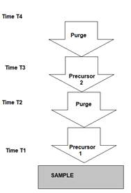
Fast-Atomic Layer Deposition Atomic Layer Deposition
Fig.7:Atomic Layer Deposition(ALD)
Comparison Table
CVD
|
PVD
|
PECVD
|
E- Beam
|
|
Advantage: ·
No line of sight deposition ·
High deposition rate ·
Mass producibility of Thick layer ·
Co deposition of multiple layers Disadvantage: ·
High temperature process ·
High Toxic precursor requirement ·
Mostly inorganic materials |
Advantage: ·
Safer process ·
Atomic level control of Chemical composition ·
No special precursor needed Disadvantage: ·
Low deposition rate ·
Thin layer deposition ·
Line of sight deposition ·
Production of only thin coating layers ·
Annealing of the film is required |
Advantage: ·
Avoids the line of sight deposition to certain
extent ·
High deposition rate ·
Low temperature deposition ·
Precursor: both organic and inorganic materials ·
Chemical and thermal stability ·
No limitation on substrates type Disadvantage: ·
Instability against humidity and aging ·
Film stress ·
Time consuming for some material structures ·
Toxic and explosive gas used in the plasma
process ·
High cost equipment |
Advantage: ·
Both metal and dielectric materials ·
Low impurity comparing to thermal deposition ·
High deposition rate Disadvantage: ·
High cost ·
High Temperature deposition |
Quick links to our main areas
(Use the regular menus to access all our other pages.)
|
Make a booking Powered by
|
News & LinksOptofab ACT newsletters Latest news - More details on our |
more
more
main news page |
|
Policy & PricingANFFL Pricing & Access Policy ACT Optofab Node Pricing details Safety & Emergency information
|
more
moremore |
|

Feedback
We run an annual User Feedback Survey but feel free to send
feedback at anytime using this form.
Providing nano and microfabrication facilities to Australia's
researchers
|
|||
|
|
|
|
|
|
Copyright 2021 ANFF Optofab ACT Node. All rights reserved. Page last updated: 30 Jan, 2021 |
|||

|
|