|
|
||||||||||||||||||||||||||||||
|
|
|
|||||||||||||||||||||||||||||
|
|
||||||||||||||||||||||||||||||
|
The ANFF is
an open access network comprising of eight Nodes across 21 institutions with
a portfolio of more than 500 tools valued at over $200 million. See: for full details |
Hybrid Integrated Optics ChipsThe
node is also offering a non-ANFF subsidised service at ANFF assisted pricing rates
(A$100/hr plus consumables costs) to produce full custom hybrid integrated
optical waveguide circuits to users. In this context, a Hybrid device is one
that incorporates a number of different materials in a single chip, each
chosen for their excellence in one or more optical processing functions. Thus
it offers a means to have passive, amplifying, optically nonlinear, etc functions on a single chip with the “best” material
chosen for each function. Whilst a flip chip bonder is available and we have
industry proven expertise and experience in bonding laser diodes to
waveguides with very high alignment accuracy, we are not currently in a
position to offer this unless you bring a supply of laser diode chips with
alignment fiducials already etched into the top contact metal due to the
costs involved in sourcing custom chips. We hope to be able to offer this
service in the future using ANU grown lasers. As far
as mixing materials on a chip goes, we achieve this via vertical tapering of
the layers during deposition which provides very low intra-material coupling
losses (<0.1 dB per junction when done properly – see images below). At
present the materials choices are: 3% index contrast Germanosilicate·
low loss and nonlinearity passive interconnects/components
·
UV Bragg
gratings and UV post tuning
·
low coupling loss to UHNA fibre
·
Library of
high performance fabrication tolerant couplers etc
·
Thermo-optic
actives with polymer cladding
Polymer waveguides (SU-8 or Polysiloxane)·
Low losses
in the sub 1 micron band down to the blue
·
Fast and
easy fabrication, direct maskless write later for
SU-8
Tantalum Pentoxide·
ultra-low loss single polarization waveguides
·
moderate nonlinearity
Tellurium dioxide (principally for rare earth doping)·
gains exceeding 4 dB/cm at 1550nm with Erbium
·
potential for SBS and acousto-optic devices
·
moderate nonlinearity
Arsenic Trisulphide/Ge-As-Se·
high nonlinearity glass for all optical processing
·
SBS based
devices
·
All
chalcogenide waveguide structures for MIR waveguide devices to 10+ microns
operating wavelength
We are also
working on technology to allow flip chip bonding in of other crystal media to
enable fast electro-optic, magneto-optic, and other functions on chip.
Ultimately this will represent all functions except detection and direct on
chip light generation, though as noted this is only a matter of money for engineering
costs. We hope that in years to come this service will be an officially
recognized and subsidized part of our ANFF offerings. Please feel free to
contact us to get more information and discuss requirements and pricing
structures.
Propagation
loss for Germanosilicate 3% delta 3 x 3um waveguide with polymer overclad for
thermo optic sections, note there is a loss tail at 1550nm and down to 800nm.
SU-8 3%
delta 3x3um polymer waveguide transmission spectrum
Er Doped
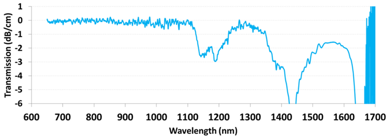
Tellurite waveguide showing low insertion/propagation loss with high doping
(Coupling losses are ~2dB here)
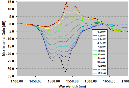
Gain in 5cm
long Er:TeO2 waveguide pumped at 980nm with lower doping than above
Vertical
Taper concept
High
nonlinearity waveguides with fibre mode matched polymer core output
waveguides using vertical taper transitions. Total chip loss for 7cm
waveguide ~3dB fibre connector to fibre connector.
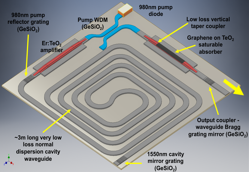
Conceptual
Hybrid integrated single chip mode locked laser
MIR
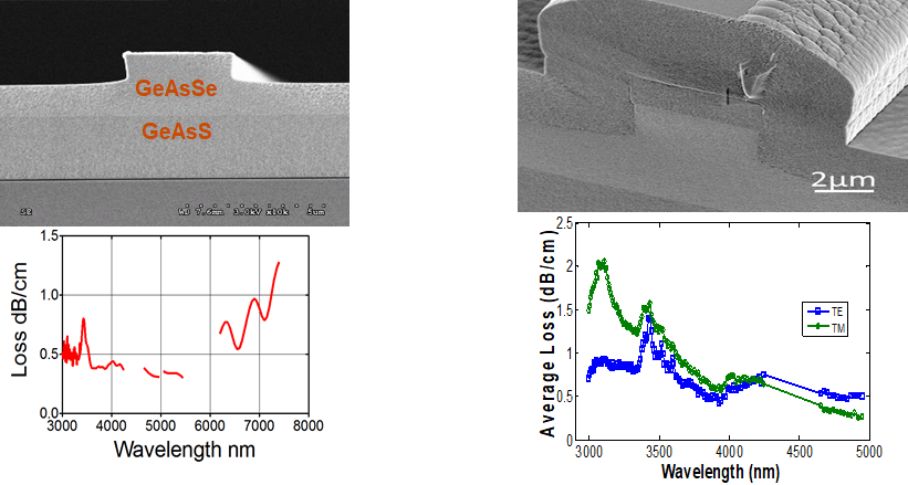
Waveguide designs and propagation losses with Ge-As-Se core and Ge-As-S
cladding. Loss slope from 3-5um is now established to be OH contamination in
Sulphur glass and all selenide solution is being developed to eliminate this.
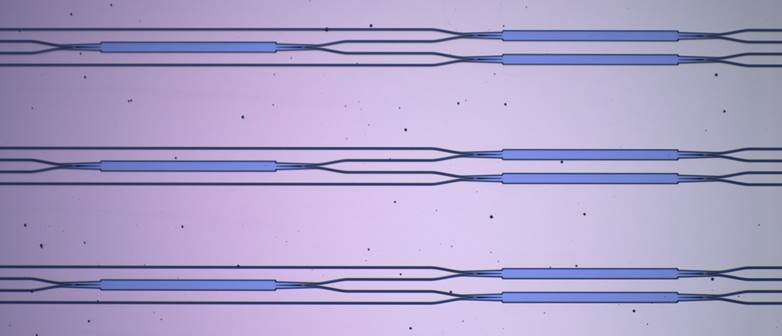
MIR coupler
network for Astronomical nulling interference application
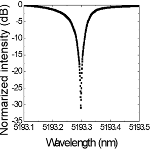
High Q MIR
ring resonator for 5um operation as chemical sensor, Q ~200,000 |
|
||||||||||||||||||||||||||||
Quick links to our main areas(Use the regular menus to access all our other pages.)
Feedback We run an annual User Feedback Survey but feel free to send
feedback at anytime using this form.
|
||||||||||||||||||||||||||||||


|
|