|
||||||||||||||||||||||||||||||
|
|
|
|||||||||||||||||||||||||||||
|
|
|
|||||||||||||||||||||||||||||
|
The ANFF is
an open access network comprising of eight Nodes across 21 institutions with
a portfolio of more than 500 tools valued at over $200 million. See: for full
details |
Tools & Capabilities – Optofab
ACT Node
For a full, searchable listing of ANFF capabilities/tools
(all 8 nodes) click here. Quick links to the following:
Thin Film Coaters
Coatings targeted at for optical and photonics applications
are our main “business” at Optofab ACT, though we
can coat for other applications also. We have six coating tools of different
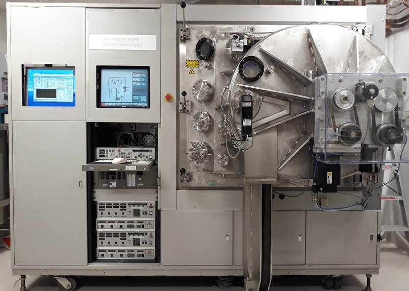
types currently available. Veeco
Spector Dual Ion Beam Sputter tool (Online)
This is an early generation Spector tool that has been
considerably enhanced by the addition of a custom door with large planetary
fixture with infinitely variable planetary ratios. The system is run in two
modes: · Standard single rotation for substrates up to 100mm (5 off max per run) which provides thickness uniformity over the 100mm diameter of ~0.3% · Dual position rotation which enables thickness uniformity <0.1% over up to 400mm diameter, though at the expense of significant reduction in deposition speed and increase in cost The substrate holder can rotate at up to 100 rpm and take substrates up to ~20Kg, up to 450mm diameter and up to 20cm thick. The chamber has a 16cm beam diameter main sputtering ion gun (up to 1200eV ion energy and 600mA beam current running on Ar or Ar+O2) that sputters off 14” targets of which 3 can be mounted and individually sputtered in a single run. The system sputters only metal oxides and nitrides meaning best performance is obtained in the visible to NIR range, though at the expense of some absorption this can be extended. Typical sputter rates in standard single rotation mode are about 1 micron per hour. The targets installed as standard are silica, tantalum, and titanium. Also available re hafnium, indium tin oxide (conductive and transparent), aluminium oxide, and tantalum nitride. Target changes take about an hour for venting, cooling system drain, target change over, and the system will pump from atmosphere to a few 10-6 Torr in 1 hour. Pumping features a soft rough to ~1 Torr to prevent “film popping” off already coated areas of the chamber and ensuing particulate generation, then fast rough to 200 mTorr, then cryo pumping. Base pressure is high 10-8 Torr, and deposition pressure is usually ~8x10⁻⁵ to 2x10⁻⁴ Torr. A 12 cm beam diameter secondary gun is used for ion assist typically with Ar + O2 feed to irradiate the substrates (standard single rotation mode only) to modify the film stress and index as deposited. Substrate heating is provided by quartz IR lamps in the chamber to a maximum of 200C during deposition. The system also has a four wavelength rotating analyser ellipsometer fitted for real time layer end pointing and film thickness monitoring on a test chip located near to the normal deposition positions. This enables extreme thickness accuracy to be achieved after appropriate calibration as the ellipsometer is sensitive to ~0.1nm changes irrespective of how many layers have already been deposited or the spectral response of the coating. In the near future, a broadband 400-1100nm white light transmission monitoring system will be added that will enable live control of layer thickness on the actual substrates to further enhance accuracy on the finished parts. There are two “standard” deposition processes calibrated on the tool: · Warm deposition: 150C deposition temperature with no ion assist, stress relieved post deposition by annealing at 550C to attain the lowest absorption losses. · Cold deposition at 25C with ion assist to aid adhesion and reduce stress (<100 MPa). Can be annealed as required. Full details regarding refractive indices for design purposes are available at: Coating
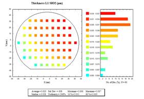
Information and Resources When used for LIGO mirrors by CSIRO, the machine was capable of producing coatings with sub 10ppm absorption in AR coatings up to ~2 microns thick, and even less in mirror stack where the absorption is reduced due to the smaller penetration into the stack. Particulate counts met the LIGO specs (~0.01/cm2) provided the shields were cleaned prior to deposition, and uniformity was <0.1% over a 400 mm diameter area, though this was not a low cost process.
DB 600 Ion assisted E-beam Evaporator (Online end 2021)
The DB 600 was a tool built by CSIRO to coat substrates up
to 600mm diameter in a stationary substrate mode using a rotating uniformity
“blade” to attain thickness uniformity to ~2%. It uses a 3 pocket electron
beam source and also has a resistively heated baffled boat source. As E-beam
evaporated coatings are often of low density and nanoporous,
the system also has an assist gun that can run on Ar
or Ar+O2 to provide compaction and densification of the films as
they grow (only on substrates mounted on a rotating holder) thereby attaining
films with good humidity stability. Substrate IR lamp heating is possible up
to ~200C. The system can deposit essentially any material, and its main
purpose at OptoFab ACT is for deposition of
Fluorides for DUV/MIR coatings which are not possible/allowable in the
Spector, and metals for metallic mirrors etc. The system has an inbuilt 6
wavelength rotating analyser ellipsometer similar
to the one on the Spector, and also a simultaneous transmission or reflection
white light monitoring systems for thickness monitoring and layer end
pointing. A wide range of coating materials is available.
Research Ion Beam Sputter tool (Online March 2021)
This is a system intended to provide low cost rapid turn around R&D on coating materials. It uses a 6cm
ion gun and a single 3-6” sputter target, these being far less costly than
the large ones used in the Spector. The system is fitted with a load lock
that accepts up to 100mm diameter substrates to enable rapid sample exchange
and allow for many sequential runs in a day under different conditions to
optimise deposition processes. There is no restriction on what materials may
be deposited in this system (with the exception of non-reactively sputtered
metals which cause arcing on the grid insulators in the gun), so cleanliness
is key here. The system has a quartz microbalance thickness monitor installed
and sputtering is performed at room temperature though an IR heater upgrade
is envisioned in the near future. At this stage the system can load only a
single target, target changes requiring vent and pump down which takes
approximately 4 hours to accomplish and reach ~2x10⁻⁶ Torr. Base
pressure is mid 10-7 Torr (turbopump limited), and deposition pressure is usually
~2x10⁻⁴ Torr.
Angstrom Engineering Evovac
Cothermal/Sputter system (Online)
The Angstrom system is primarily used for photonics films applications and has six Radak resistively heated evaporation sources installed using quartz, ceramic, or metal crucibles, and a further baffled boat option as well. Each source has its own quartz microbalance rate monitor enabling the system to monitor the deposition rate through software. The machine is capable of co-evaporation of different materials and so far two kind chalcogenide glasses deposition is well established process for three layers deposition without any vacuum break. Also some experiments were carried out to perform the co sputtering and co evaporation of different materials. The following materials are evaporated and sputtered using this tool: Ge11As24.5Se64.5, Ge11As24.5S64.5, Sb2S3, As2Se3, Ge, Ga, Se, S, SiO2, TeO2, GLS, Er2S3 etc. The equipment is capable of handling four 100mm wafers at a time, however we can also deposit on the nonstandard wafers or samples as per customer request. Thickness capability is from less than 100 nm to few tens of micron.
To make a booking for thermal and sputtering evaporation Click here
Octal Thermal Evaporator (Online)
The Octal Thermal evaporation system is restricted to depositing very low optical loss sulphur based chalcogenide films for which it is the “production” tool. The system can handle four wafers of 4 inch circular size at a time. The system uses SiO coated Ta baffle box to heat the materials for thermal evaporation. To control the process of deposition and contamination, Residual Gas Analyser (RGA) is used to monitor the process during the deposition. The thickness capability of the tool ranges from less than
100 nm to 20 um at less than 10 Angstrom per second deposition rate.
To make a booking click here
Pfeiffer DC Sputter tool (Under repair)
This system uses a single 6” diameter sputter target
(Chromium or Aluminium Currently available) and a DC discharge to deposit
metal films on substrates up to 150mm diameter.
Canon
MPA-500 FAB 1:1 Projection Aligner (Online)
The MPA-500 aligner operates in broadband exposure mode only on 100mm or 4” wafers using 5” mask plates. The “MPA” stands for Mirror Projection Aligner and so the optics is completely achromatic being reflector based so the broadband exposure is not an issue in resolution terms and in fact speeds up exposure using more of the 2kW arc lamp spectrum. The tool operates based on the realisation by Perkin-Elmer that a 1:1 spherical mirror relay system has an arc of diffraction limited performance, and so this arc is scanned over the mask and projected to the wafer at 1x magnification. Being a scanning system, exposure uniformity is excellent, and the UDOF is ~4 microns at the production “limit” of 1.5mm Line-Space patterns. For isolated features we have patterned down to about 800nm. The system has a standard split field microscope manual alignment system using stepper motors, but also a laser scanning auto-alignment system using proprietary “V” alignment markers that provides +/- 100nm overlay alignment in a couple of seconds. Wafer loading is either manual or to/from standard H bar wafer cassettes, and typical exposure times for 1.um thick Clariant AZ MIR-701 positive resist are in the 20-30s vicinity so throughput can be quite high if large batch sizes are needed. Repeatability and precision overlay are the main benefits of this tool, as well as maintaining photomasks in good condition.
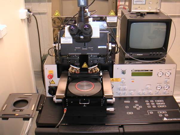
Karl
Suss MA-6 Contact/proximity Mask Aligner (Online)
The MA-6 mask aligner operates in I-line mode currently only on 100mm or 4” wafers. Under ideal circumstances with very clean substrates and masks, we have printed sub 0.5um features on this system, but its resolution is essentially limited by substrate quality. Normally 2um features are not difficult with silicon wafers in soft contact mode and a good high resolution resist (we use Clariant AZ MIR-701). Typical exposure intensity is around 2-4 mW/cm2 in I-line mode depending on lamp age and condition of the reflective collimator in the 350W arc lamp source, leading to exposure times typically around 1 minute for 1um thick Clariant AZ MIR-701. The system has a split field microscope and manual large diameter micrometers for overlay alignment, but if using contact printing this limits the routinely achievable overlay accuracy to ~1um.
Dover Vector Optical Writer (under rebuild)
The Dover air bearing system is an XY stage system with 10nm precision over 150mm of motion range. It is paired currently with a blue laser diode system that can generate a programmable light pattern that is used to draw on photoresist with a high numerical aperture low distortion objective by moving the stage. This is of particular value for waveguide circuits as the stage can also draw true non discretised curves meaning lower roughness and waveguide losses. Once established with blue light the longer term plan is to upgrade to 200 nm illumination and exploit the inherently lower line edge roughness of ArF 197 nm photoresists for very high performance waveguide devices down to 500nm widths. Major advantages of this methodology are rapid prototyping, no sunk reticle costs (expensive for steppers) and vastly lower cost of ownership than an ArF stepper.
SVG 8600 series coat and develop lith track
(Online)
The Silicon Valley Group 8600 series lithography track is a
fully automated H bar cassette to cassette photoresist coat and develop
system for wafers from 50mm to 150mm diameter. It has a single high
resolution I line positive resist permanently plumbed in (Clariant
AZ MiR 701) with an automated dispense arm, a
pressurized canister dispense for adhesion promoter, and a positive
displacement syringe pump style dispense to enable coating of any other type
of resist or dielectric spin on coat. It can spin at speeds from 50 rpm to
10,000 rpm, run up to 10 steps in a process, and also features programmable
back side wafer cleaning and topside edge bead removal. Under ideal
environmental conditions it is capable of 4nm repeatability any point on any
wafer to any point on any other wafer. After coating, the wafer can be softbaked up to 200C on the proximity or vacuum contact
hotplate with programmable decent and rise parameters. Development is via
either static puddles or dynamic streaming with up to 10progammable steps,
followed by a DI water spray rinse and spin dry. Hardbake
is again available up to 200C, and Post Exposure baking can be accomplished
by programming a null program on the coater or developer module.
Repeatability and uniformity are the greatest attributes of this equipment,
especially crucial for lithography.
Hot-embossing with soft
stamps (On request)
The homebuilt thermal NIL tool offers the possibility of creating sub-µm structures in materials with softening temperatures to ~400C using a PDMS mould. Lateral resolution is down to 200 nm. Patterning can be done on substrates up to 100mm diameter. Please contact us to discuss any needs you may have.
UV-Nanoimprint Lithography (Online)
Oriel UV Flood Exposure System (Online)
The Oriel Flood exposure unit provides flood exposure services at >10 mW/cm2 for a wide variety of applications. It uses a 1200W Hg-Xe lamp and a paraboloidal reflector in conjunction with homogenization optics to achieve high uniformity and short exposure times on wafers up to 150mm diameter. A nitrogen purged exposure chamber is available for use with many of the UV curing materials used as glues or overcoats that will not cure in the presence of Oxygen.
Raman System (under rebuild)
Homebuilt Raman system based on Olympus Microscope and
Ocean Optics Deep cooled CCD array spectrometer using 800nm pump source.
Can measure sub-micron thick films with low noise!
Olympus Microscope and high res camera (Online)
The Olympus BX60M microscope is equipped with objectives from 5x to 100 x 0.9NA and a 3500 x 2000 pixel monochrome camera and image acquisition software. Will be fitted with motorised programmable stage for area image acquisition and defect mapping by October 2020. Offers Brightfield, Dark Field, Normaski Differential Interference Contrast all in reflection only. Blue cut filter installed to enable observation of photoresist.
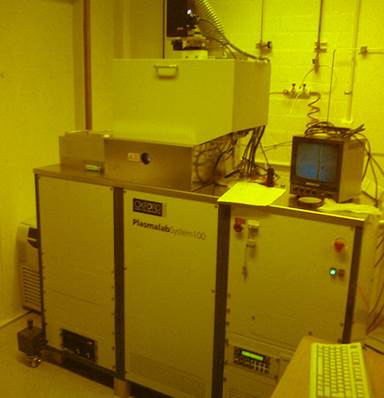
Inductively Coupled Plasma Etching - Silicon and
Dielectrics (Online)
The ICP-RIE (Oxford PlasmaLab 180
series) features a load-lock, a temperature controlled etch table (0-90C), He
backside cooling and sample size up to 6” substrates. Table power is up to
500W, ICP power to 3 kW.
Capability: Si based (Si, SiO2& Si3N4), oxides (ITO, TiO2, TeO2, Ta2O5, ZnO, etc), polymers (BCB, SU-8, Polysiloxanes, etc)
Barrel Etcher - PVA TePla (Under Repair)
A high pressure plasma system to descum and strip resists in O2-plasma and other organic materials.
The low power feature allows footage removal after resist development to obtain clean patterns.
With the addition of CF4 combined stripping of resists and SiNx/SiOx is possible.
This machine is capable of handling up to two 4" wafers or one 6" wafer.
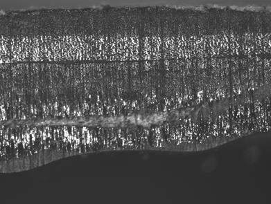
SCI Filmtek 4000 Wafer Mapper (Online)The FilmTek 4000 is a computerised, non-destructive material characterisation system that provides very high accuracy, easy of use and analytical power in fully integrated package. This software controlled equipment combines Fiber optic spectrophotometry with advanced material modelling software to provide an affordable and reliable tool for simultaneous measurement of various parameters of thin film. The equipment uses SCI’s patented Differential Power spectral Density Technique (DPSDT) to calculate the thickness and refractive index of the measured films by collecting the normal incident and polarised 70 degree reflection data. Reflection data is obtained by comparing the sample data to the measured reflection of a known reference sample typically a silicon wafer with a thermally grown thin oxide film. Using generalised material models in combination with global optimisation algorithms and power spectral density analysis (DPSDT), FilmTek can simultaneously determine the following parameters of the materials: Multiple layer thickness Indices of refraction vs wavelength Extinction coefficients Energy Band gap Surface roughness All the above mapped across a 6” wafer Filmtek 4000 can measure virtually all translucent film thickness ranging from less than 100 angstrom to 250 um. The key features of the tool are index measurement resolution up to 2x10⁻⁵,multi angle, polarised spectroscopic reflection (350nm to 1700nm), automated stage for wafer mapping, autofocus and Auto beam alignment, Camera for imaging measurement location. Typical application of the filmtek is as follow: Semiconductor and dieletric materials Planar Integrated waveguide materials Optical antireflection coatings Coated glass Electro optic materials Multilayer optical coatings SOI or SOS materials Resin thickness in CD or DVD etc
Wafer Map of As2S3 Layer on 5 um Thermal Oxide wafer:
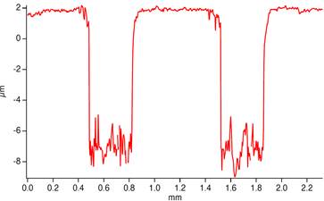
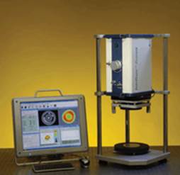
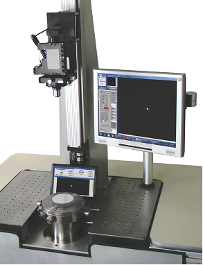
Wyko NT9100 Profilometer (Online)The benchtop Model NT9100 optical surface profiler is a very convenient, high performance non-contact 3 dimensional metrology tool. This tool provides superior non-contact measurements on the widest variety of super smooth or very rough surface samples from sub nanometer surface roughness to millimetre high steps. It has been designed to provide highly reliable and repeatable tabletop characterisation for R&D, wear, failure analysis, process control and process monitoring. Height maps can be taken of an individual image or multiple images automatically acquired and stitched together. The specification of the Equipment is as below: Objectives 5X, 20X, 50X, (100x on request) Through Transmissive Media 5x objective. Field-of-View Multipliers 0.55X, 1X, 2X Measurement Array 640 x 480, non-interlaced Light Source Long-lifetime green and white LEDs Optical Assembly Dual LED illuminator; Three-position FOV turret, closed-loop, 10mm scan Stages Automated 100mm Z-axis; ±6° tip/tilt stage; 150mm XY auto stage Software Vision running under Microsoft® Windows XP® Professional;
Production mode, built-in databasing with pass/fail
for any parameter; Optional Stitching, MATLAB/TCPIP, Film Analysis, Optical
Analysis, and SureVision Vertical Measurement 0.1nm to 10mm std. Range Vertical Resolution <0.1nm RMS Repeatability 0.05nm Vertical Scan Speed User-selectable up to 24μm/sec Lateral Spatial Sampling 0.1 to 13.2μm Optical Resolution 0.49μm min with 100x 0.8 NA lens. Field-of-View 7.68 x 5.76mm max, 0.06 x 0.05mm min with std-resolution cameraReflectivity <1 to 100% Step Height 0.8% accuracy and less than 0.1% 1 sigma repeatability
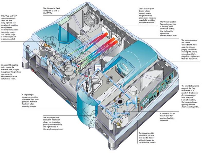
Cary 5000 Spectrophotometer (Online)
The Cary 5000 is a spectrophotometer covering the range
175-3300nm based on a dual grating monochromator
(switchable UV-Vis and IR gratings) and photomultiplier/Lead Sulphide
detectors. The UV-Vis arrangement provides optical resolutions of 0.01-5 nm
and the IR 0.05-5 nm. The instrument has independent but simultaneously
measured sample and reference beam paths with a log ratio amplifier comparing
the outputs if desired. The log ratio amplifier has about a +/- 5 decade
range, so to obtain high dynamic range (OD6+) attenuation of the sample (or
rear) beam is required. There is a trade off here
between dynamic range and noise on the 100% transmission level, you need to
choose which is more important to you! With no rear beam attenuation, the
spec on noise at 100% transmission is 0.00003 Abs units. The machine comes with an automated Rear
Beam Attenuator which provides up to OD 1.7 attenuation for the reference
path which is sufficient for exceeding OD6 across the whole spectral range.
Under ideal conditions, the machine can reliably measure OD10 in the visible
(we plan to perform proof test for the full range in the near future) and OD
8 in the IR (again full range to be explored). The machine has inbuilt
Deuterium and Mercury lamp sources so is able to self
calibrate for wavelength based off a primary reference atomic source
and is therefore certifiable. The spec on wavelength accuracy is +/- 0.1nm
for UV-Vis and +/- 0.4nm for IR. The system has a large sample compartment
can can also be configured to measure large
diameter substrates as long as their thickness does not exceed ~12 cm. Aside from simple transmission measurements, the instrument has a variety of attachments of which the most relevant to optical devices are the Absolute Specular Reflectivity (SRA) and Variable Angle Specular Reflectivity (VASRA) attachments. The former uses a single reference mirror of known reflectivity to reference close to normal incidence reflectivity in both the signal and reference paths, thereby allowing a user’s mirror to be evaluated in absolute reflectivity terms. It can also compare two mirrors. The VASRA is intended for measuring reflectivity at different angles from 20 to 70 degrees, polarized or unpolarised and is fully automated.
Supercontinuum and OSA (Online)
The supercontinuum source is a single mode photonic crystal fibre based source pumped at 1064nm by a high pulse energy picosecond long cavity laser. It produces about 400mW of light with a spectrum spanning ~400-2200nm with a relatively flat and temporally stable spectrum. It can be used with either our Ando AQ 6317 or Agilent 86140B optical spectrum analysers to make spectrally resolved measurements of fibre coupled devices (single mode or multimode), or free space components through use of one of our fibre “U benches” with no alignment necessary. The high source power enables measurements of loss down to about 60dB across most of the spectrum with this reducing the deeper the measurement goes into the visible region. A software control panel that enables trace dumping to disc and full control over the OSA is also available. Mapping T & R System
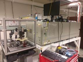
This custom-built setup can autonomously measure the transmission and reflection of substrates up to 400mm in diameter. Its XY-translation stage allows for a full 2D high resolution scan at pre-set angles of incidence (angular range is subject to substrate thickness). An optical chopper modulates the laser intensity and low-noise lock-in amplifiers isolate the reflection and transmission signatures in the photodetector signals. The absolute magnitude of reflection and transmission is evaluated against calibration optics. Currently, only wavelengths of 532, 633 and 1064nm can be supported due to laser availability, but additional wavelengths may be made available on request. Optical Absorption System
This custom-built setup uses photo-thermal common path length interferometry to measure the absorption of thin-film coatings. A strong, focused pump beam causes spot heating in the coating on the optic under investigation. The amount of heat deposited scales with the pump beam power and the absorption in the coating. Due to the thermo-optic coefficient of the substrate material, a thermal lens is formed that causes wavefront aberrations of a low power probe beam which samples the heated area. The pump beam is optically chopped, such that the wavefront aberrations are modulated with the change of pump intensity. An apertured photodetector, or alternatively an array wavefront sensor, captures the modulation signal, whose magnitude is calibrated against samples with known absorption. Currently, only absorption measurements at 1064 nm are supported due to laser availability. The setup is able to perform line scans of the optical absorption and upgrades to record a 2D map are in progress. Moore
Nanotech UPL 250 Single Point Diamond Turning Lathe
The Moore Nanotech 250 UPL lathe has precision four-axes control (Y-Axis, Z-Axis, rotary B-Axis, C-Axis positioning) with a stiff air-bearing spindle. It can fabricate non-cylindrically symmetric optical components with size ranging from tens of micrometres to the maximum work piece capacity of 300 mm diameter x 200 mm long (150 mm diameter swing capability over the optional rotary B-Axis). Normally it is used for the rapid production of spherical & aspheric optical lenses, mirrors, mould inserts, freeform optics, and even mechanical components. Depending on the material and the complexity of the form, surface smoothness of up to λ/50 may be attainable.
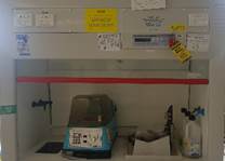
Chalcogenide Glass Fabrication
Laboratory
The chalcogenide glass lab enables us to synthesis high quality chalcogenide glass with different compositions, such as As-S, As-Se, Ge-As-Se, Ge-Sb-Se, Ge-Se-Te etc., via melt-quenching technique. We are able to fabricate chalcogenide glass rods with diameter ranging from 6 mm to 50 mm, length up to 100 mm.Chalcogenide glass dicing and polishing services are also available in glass fabrication lab.Chalcogenide glasses with customised composition/properties can also be designed and synthesised after consulting with our experienced technician.
Differential Scaling Calorimeter
The Flash DSC1 from Mettler Toledo can be used to analyse changes in the microstructure of metastable materials, to optimize the composition of materials, to simulate technological processes, and for the thermal analysis of very small samples. This equipment includes the following features: Ultra-high cooling rates: 0.02 to 50K/min Ultra-high heating rates: 0.02 to 300K/min Wide temperature range: RT to 500 °C Sampling rate: maximum 50 values/second Fast-response sensor and high sensitivity
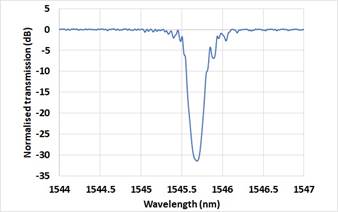
248nm Excimer Laser Bragg Grating Writing
System
GSI Lumonics, IPEX 848 The IPEX 848 Industrial excimer lasers can be used for precision applications in electronics, telecommunications, semiconductor, medical devices and pulsed laser deposition. Specifications: Wavelength: 248nm (KrF) Average power: 80W Stabilised pulse energy at maximum repetition rate: 400mJ Maximum pulse energy: 450mJ Repetition rate: 0-200Hz Pulse duration: 12-20ns
MID IR
Lab
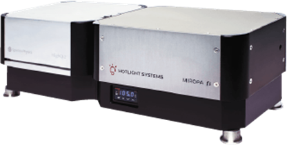
Daylight Solutions CW tunable Quantum Cascade Laser The water-cooled EC-QCL from Daylight Solutions (model 21052-MHF) is a CW MIR laser source. The operation wavelength is tunable form 5.04 μm to 5.47 μm, with an output power ~100 mW. Daylight Solutions MIRcat-1400 Pulsed Tunable Quantum Cascade Laser Daylight solution MIRcat-1400 covers the emission range of 6-13.6 μm, and the max average power is 50 mW. The pulse duration is 40 to 500 ns (20 ns increments) and the pulse repetition rate is from 0.1 kHz up to 100 kHz. IPG Photonics Cr:ZnSe CW Laser CLT-2500/400-0.05-SF laser system from IPG Photonics is a high power CW, single frequency MIR laser operating at the centre wavelength of 2300nm and tunable over 2120nm to 2600nm, with the output power of up to 1.8W (depending on wavelength and pump power set point). Picosecond OPA system The home-built picosecond OPA system uses an ytterbium pump laser and three tunable continuous wave (CW) semiconductor lasers which are combined in a MgO doped periodically poled lithium niobate (MgO:PPLN) crystal. The typical output from the OPA is 8 ps pulses at a repetition rate of 21 MHz and 200 mW of average power at 4 μm. The tunable range of this OPA can cover the wavelength from 3-5 μm. MIROPA system MIROPA system is a compact quasi-continuous femtosecond mid-infrared source based on a seeded optical parametric amplifier design. The output from this system is ~200fs pulses with average power of 200mW, and the tunable range for this system is 3-4.6 μm.
The lab is also equipped with a 1-5 mm Xenics Onca cooled InSb camera, a Xenics Gobi 4-17mm microbolometer camera, an Oriel Cornerstone monochrometer with gratings covering the 2-20 mm range, Oriel and Agilent FTIR spectrometers, calibrated high linearity pyrometer detectors, HgCdTe detectors covering the range 2-16 mm (all cooled some to -40C some to liquid nitrogen), a fibre/waveguide coupling bench, etc. Nabertherm 600 C Oven
Electrically heated air circulation furnace 415V 27 A 19KW Temp max 650 deg C Atmosphere Air, humid air controlled by bubblers, Nitrogen Vacuum low limit Atmospheric pressure Chamber volume 250 liters Programmable Yes Feature Gas inlet Very uniform temperature all over the big chamber thanks to a fan on the back that circulates air -> +/- 4 degC @ 600degC Exhaust on top of the furnace can capped with a lid Datalogging of Temp inside chamber plus Temp and RH outside furnace
1100C 6” Tube Furnace
240V 46A 11KW Temp max 1100 degC Atmosphere Air, N2 and Ar Vacuum low limit Atmospheric pressure Chamber volume Accepts up to 4-inch wafers Programmable Yes Features Room for 75 4” wafers in the tube
High vacuum ovens (600C at 10-6 Torr)
Temp max 600 degC Atmosphere Air Vacuum low limit 10-6 Torr Chamber volume ~ 50L Programmable yes Features Windows on the front and back of the oven facing each other Water cooling system
Cascade Tek vacuum oven
Temp max 300 degC Atmosphere Air Vacuum low limit 20 mTorr Chamber volume 48l Programmable yes Features Temp uniformity +/- 7% @ 150 degC
Thermoline Vacuum Oven
240V 800W Temp max 200 degC Atmosphere Air Vacuum low limit 20 mTorr Chamber volume 40l Programmable yes
Heraeus T6060Drying oven with natural convection Temp max 300u Atmosphere Air Vacuum low limit Atm Chamber volume 57l Programmable yes Features Temperature deviation +/- 6 degC @300 degC
Metricon 2010 Prism coupler (Under repair)
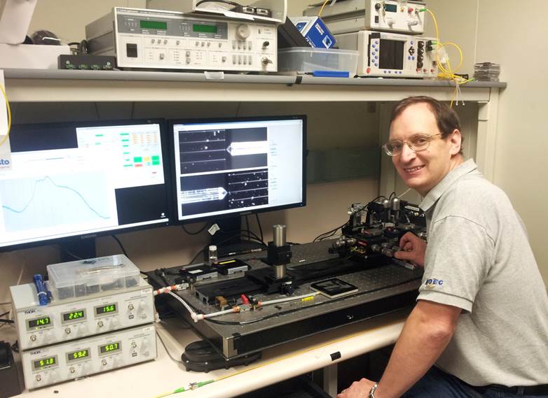
Metricon 2010 prism coupler offers an accurate way of measuring the refractive index of film/bulk glass as well as the thickness of optical films. The wide refractive index measurement range covers from 1.95 to 3.35. The worst index accuracy is ±0.0005, and the thickness accuracy is ± (0.5% +/- 5 nm). The operation wavelength covers visible (532nm, 632nm and 780 nm,) and NIR (980 nm, 1310 nm and 1550 nm) range, and two detectors (Silicon and Germanium detectors) are optional to match the wavelength. Coupled with our InGaAs camera, loss streaks can be recoded and film or waveguide propagation losses measured using custom Labview software. Waveguide Test lab (Online)
|
|
|
|||||||||||||||||||||||||||
Quick links to our main areas(Use the regular menus to access all our other pages.)
Feedback We run an annual User Feedback Survey but feel free to send
feedback at anytime using this form.
|
|
|||||||||||||||||||||||||||||


|
|